
Proton Beam Writing
Micro- and nano-fabrication are cutting-edge technologies that are at the forefront of modern scientific research and industrial innovation. These processes involve the design and creation of devices and structures with dimensions that are measured in micrometers or nanometers—one micrometer being one-millionth of a meter and one nanometer being one-billionth of a meter. This level of precision enables the development of highly advanced materials and systems with applications across various fields including electronics, medicine, and energy. [1, 2]
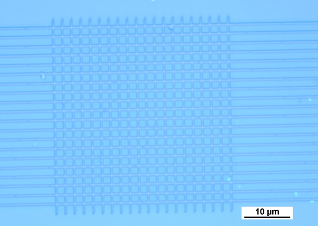
Optical Microscope Image of Nanoscale Chromium Grid on Glass: After patterning and depositing metal, a nanoscale grid is fabricated
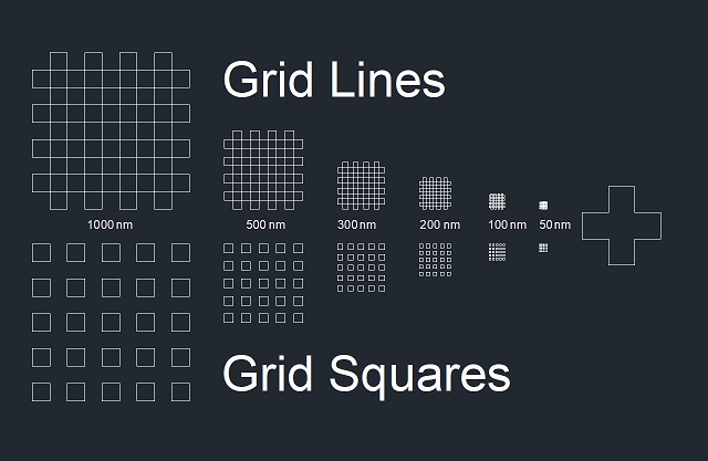
Exposure Matrix Drawing: Matrix of different sized features are first designed
At CIBA, we specialise in the intricate world of micro- and nano-fabrication, pushing the boundaries of what’s possible in miniaturization. Our state-of-the-art facilities allow us to do Proton Beam Writing, enabling us to produce microchips, sensors, and other components that are essential for the next generation of technological advancements. [3, 4, 5]
The techniques we employ in micro- and nano-fabrication are diverse and sophisticated, ranging from lithography, which allows us to etch fine patterns onto substrates, to deposition processes that build up materials layer by layer to form the desired structures. Our researchers and engineers are dedicated to refining these techniques and developing new methods to overcome current limitations of proton beam writing, ensuring that our research centre remains at the leading edge of the micro- and nano-technology.
References
| [1] | C. Koch and T. J. Rinke, Photolithography: Basics of Microstructuring. Ulm, Baden-Württemberg: MicroChemicals, 2020. |
| [2] | S. Cabrini and S. Kawata, Nanofabrication Handbook. Boca Raton, Florida: CRC Press, 2012. |
| [3] | J. A. van Kan, P. Malar, and Y. H. Wang, “Resist materials for Proton Beam writing: A Review,” Applied Surface Science, vol. 310, pp. 100–111, 2014. doi:10.1016/j.apsusc.2014.04.147 |
| [4] | J. A. van Kan, A. A. Bettiol, and F. Watt, “Three-dimensional nanolithography using proton beam writing,” Applied Physics Letters, vol. 83, no. 8, pp. 1629–1631, 2003. doi:10.1063/1.1604468 |
| [5] | J. A. van Kan et al., “Proton beam writing: A platform technology for nanowire production,” Microsystem Technologies, vol. 14, no. 9–11, pp. 1343–1348, 2008. doi:10.1007/s00542-007-0514-y |
Content by Ryan Yang, 2023