Abstract:
Modifying and manipulating properties of 2D materials is central for achieving the potential of these materials. In our group we aim at synthesizing 2D materials by molecular beam epitaxy and study approaches for controlled modifications by alloying, doping, one-dimensional modifications (edges or grain boundaries) or interfacing with dissimilar materials. In the first part of the talk we present our studies on the formation of metallic mirror twin grain boundaries in MoSe21 or MoTe22 by incorporation of excess Mo into the lattice (see Figure). Very high density of MTB networks can be obtained in MoTe2 that effectively metallizes the material and thus may act as a metallic contact patch.3 Such line defects may also increase electrocatalytic properties for hydrogen evolution reactions.4 On a more fundamental level, we show that these 1D metallic grain boundaries host a one-dimensional electron gas and we present the first angle resolved photoemission (ARPES) studies of the electronic properties of such line defects. These studies show evidence for the presence of Tomonaga-Luttinger Liquid behavior.5 The second part of the talk focuses on the differences in charge density wave properties of metallic TMDCs in the monolayer compared to bulk materials. Here we focus on the layer dependent variations of the properties of VSe26 and VTe2.7 For both materials we observe a charge density wave (CDW) behavior in the monolayer limit compared to their bulk properties. From ARPES and DFT we can also show that CDW competes with ferromagnetic ordering in monolayer VSe2.6 In VTe2 we observe a structural transition from a distorted-1T’’ structure in the bulk to a simple hexagonal 1T structure in the monolayer. This structural transition is accompanied by a CDW instability for the monolayer that gives rise to a 4×4 CDW at low temperatures, in contrast to bulk VTe2 that does not exhibit a CDW instability.7
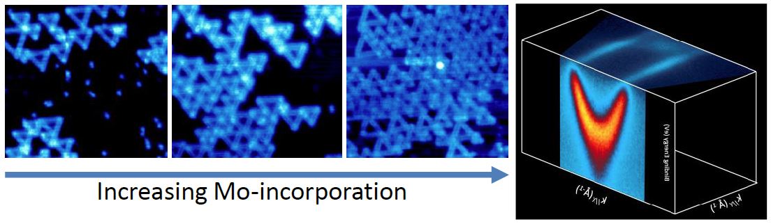
Figure: Line defect formation in 2H-MoTe2 with increasing Mo-deposition and the defect-induced band gap states measured by ARPES, showing linear (1D) Fermi-surface and dispersing bands.
References:
- Y Ma, S Kolekar, H Coy Diaz, J Aprojanz, I Miccoli, C Tegenkamp, M Batzill. Metallic Twin Grain Boundaries Embedded in MoSe2 Monolayers Grown by Molecular Beam Epitaxy. ACS Nano 11, 5130-5139 (2017)
- HC Diaz, Y Ma, R Chaghi, M Batzill. High density of (pseudo) periodic twin-grain boundaries in molecular beam epitaxy-grown van der Waals heterostructure: MoTe2/MoS2. Appl. Phys. Lett. 108, 191606 (2016)
- PM Coelho, HP Komsa, H Coy Diaz, Y Ma, AV Krasheninnikov, M Batzill. Post-Synthesis Modifications of Two-Dimensional MoSe2 or MoTe2 by Incorporation of Excess Metal Atoms into the Crystal Structure. ACS Nano 12, 3975-3984 (2018).
- T Kosmala, H Coy Diaz, HP Komsa, Y Ma, AV Krasheninnikov, M Batzill, S Agnoli. Metallic Twin Boundaries Boost the Hydrogen Evolution Reaction on the Basal Plane of Molybdenum Selenotellurides. Adv. Energy Mat. 1800031 (2018).
- Y Ma, et al. Angle resolved photoemission spectroscopy reveals spin charge separation in metallic MoSe2 grain boundary. Nature Commun. 8, 14231 (2017).
- P Coelho et al. Charge Density Wave State Suppresses Ferromagnetic Ordering in VSe2 Monolayers. J. Phys. Chem. C 123 14089-14096 (2019).
- P Coelho et al. Monolayer Modification of VTe2 and its Charge Density Wave. J. Phys. Chem. Lett. 10, 4987-4993 (2019).