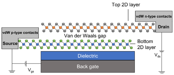
Exploitation of fundamental properties of atomically thin (two-dimensional, 2D) semiconductors – particularly those from the transition metal dichalcogenide (TMD) family – for electronics will require ultra-clean contacts with resistances approaching the quantum limit. The lack of high quality, low contact resistance p- and n-type contacts on 2D semiconductors has limited progress in next generation of low power devices such as the tunnel field effect transistors. In this presentation, we summarize strategies and provide guidance for making clean van der Waals (vdWs) contacts on mono-layered semiconductors. I will then present our recent work on using vdW gap as tunnel barrier for spin injection and collection in graphene using ferromagnetic contacts.
Biography
Prof Chhowalla, FREng, is the Goldsmiths’ Professor of Materials Science at the University of Cambridge. His research interests are in the fundamental studies of atomically thin two-dimensional transition metal dichalcogenides (TMDs). In particular, his group studies the optical and electronic properties of different phases of 2D TMDs. He has demonstrated that it is possible to induce phase transformations in atomically thin materials and utilize phases with disparate properties for field effect transistors, catalysis, and energy storage. Prof Chhowalla is a Fellow of the Materials Research Society, Institute of Physics, the Royal Society of Chemistry and Churchill College. He was the founding Editor in Chief of Applied Materials Today and is now the Associate Editor of ACS Nano.