
Email: mirsaidov@nus.edu.sg
Office: S1A-02-11
Tel: +65 6516 6192
Current Research
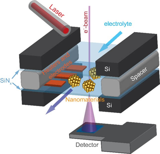
- The broad goal of our research program is to understand the underlying mechanisms of chemical and physical processes involved in the fabrication and application of nanomaterials. We study nanomaterials critical for future microelectronics and renewable energy sources. To gain mechanistic insight into the fundamental physical and chemical processes, we use in situ liquid-phase, gas-phase, electrochemical, and cryogenic transmission electron microscopy (TEM) imaging approaches along with other complementary techniques. Our approach enables us to visualize many elusive nanoscale processes in real-time directly, allowing us to identify rapid transient stages in many materials-related processes.
- Currently, we are working on three broad topics:Addressing challenges in the semiconductor industry: Processes development for overcoming scaling issues. The key challenge confronting the microelectronics industry is conforming to Moore’s law by increasing the density of transistors on a chip using high-aspect-ratio 3D nano-architectures. While increasing device density by packing devices into 3D nano-architectures can address the scaling issue, 3D architectures pose new fundamental challenges in terms of fabrication. In current fabrication processes, liquid or gaseous chemicals etch, grow, clean, and coat the wafer surfaces on which nanometer-size features are progressively fabricated. Today, we write nanoscale patterns over large 2D areas using lithographic processes. However, the ability to write the nanoscale patterns does not directly translate into the chemical ability to fabricate 3D structures at the same length scales because of the failure modes in etching, growing, and cleaning of vertical nanostructures. To understand and improve the nanoscale processes associated with the fabrication of vertical channel materials (in transistors) and ‘scaling boosters’ in metal interconnects (device packaging), we first have to visualize them and pinpoint the possible intermediate stages that lead to their failure during the fabrication. Our goal is to identify mechanisms in semiconductor fabrication-related processes by taking a very direct approach to image nanostructures (used in device fabrication) in real-time as they are undergoing relevant chemical or physical processes encountered in the semiconductor industry.
Insight into catalytic processes by identifying the link between function and structure. During catalysis, the dynamical structure of a nanoparticle catalyst, which only exists within the reactive environment, determines the availability of active sites on its surface, which in turn determines its catalytic properties. However, how nanoscale catalysts change their structure under reaction conditions and become catalytically active is poorly understood and hotly debated. The lack of understanding here is mainly due to the challenge of observing the nanocatalysts during a gas or liquid phase reaction at elevated temperatures. Our goal is to establish the function–structure relation (activity vs. catalyst’s surface structure) by studying the surface of catalysts and the interface between the catalysts and support material.
Mechanistic understanding of nanomaterials synthesis: Nanomaterials with different architectures (shape, structure, and materials composition) are commonly synthesized from precursor solutions through one-pot reactions, seed-mediated synthesis, or the reshaping of template nanoparticles. Currently, nanomaterials synthesis still remains an art based on well-tuned recipes that are derived from laborious trial-and-error approaches. Our goal is to determine the fundamental underlying chemical and physical processes that govern the formation of nanomaterials from the solution phase and provide a rational route to synthesis using direct real-time TEM imaging.
Selected Publications
- I. Erofeev, Kh. Saidov, Zh. Baraissov, H. Yan, J.-L. Maurice, F. Panciera, and U. Mirsaidov, “3D Shape Reconstruction of Ge Nanowires During Vapor-Liquid-Solid Growth Under Modulating Electric Field.” ACS Nano 18(34), 22855–22863 (2024).
- W. Wang, I. Erofeev, Y. He, F. Yang, H. Yan, J. Lu, U. Mirsaidov, “Direct Observation of Hollow Bimetallic Nanoparticle Formation through Galvanic Replacement and Etching Reactions.” Nano Letters 23(23), 10725–10730 (2023).
- Y. Jiang, M. Duchamp, S.-J. Ang, H. Yan, T.-L. Tan, U. Mirsaidov, “Dynamics of Fcc-to-Bcc Phase Transition in PdCu Alloy Nanoparticles.” Nature Communications 14, 104 (2023).
- T. Ghosh, J. Arce-Ramos, W. Li, A. Genest, H. Yan, S. W. Chee, A. Genest, U. Mirsaidov, “Periodic structural changes in Pd nanoparticles during oscillatory CO oxidation reaction.” Nature Communications 13, 6176 (2022).
- U. Anand, T. Ghosh, Z. Aabdin, S. Koneti, X. M. Xu, F. Holsteins, U. Mirsaidov, “Nanoscale Wetting of Patterned Surfaces.” Proceedings of National Academy of Sciences U.S.A. 118(38), e2108074118 (2021).
- X. Liu, S.-W. Chee, S. Raj, M Sawczyk, P. Kral, U. Mirsaidov, “Three-Step Nucleation of Metal-Organic Framework Nanocrystals.” Proceedings of National Academy of Sciences U.S.A. 118(10), e2008880118 (2021).
Affiliations & Links
- Department of Biological Sciences
- Centre for BioImaging Sciences
- Mirsaidov Lab